Hotline:0755-27247642
Consult immediatelyThe circuit board leads the military industry12 years focus on high-precision circuit pcb, fpc manufacturers
Hotline:0755-27247642
Consult immediatelyThe circuit board leads the military industry12 years focus on high-precision circuit pcb, fpc manufacturers
Shenzhen CengFengElectronics Co., Ltd.
Factory address: Shenzhen City, Baoan District Songgang town Yanchuan Dahua Feijie Science Park 2 4 floor
Telephone: 0755-27247642/27247955
Technical support: Mr. Liu, 13428714088
Fax: 0755-85244605
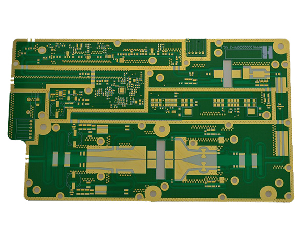
Determination of size and shape of 1.PCB
First of all, according to the mechanical structure of the product. When the space location is more abundant, we should try to select a small area of PCB. Because the area is too large, long printed lines, increased impedance, noise resistance, cost increases, but also take full account of the components of heat dissipation and adjacent to the line, easy to interference and other factors.
2. layout
Layout principle of special components
Shorten the connection between the high frequency components as much as possible, and try to reduce their distribution parameters and electromagnetic interference between them. Vulnerable components should not be too close to each other, and input and output components should be kept as far away as possible.
Second, some components or wires may have higher potential difference, should increase the distance between them, so as not to discharge lead to unexpected short circuit. The components with high voltage shall be arranged as far as possible when the hand is not touched at the time of debugging.
Parts weighing more than 15g shall be fixed with brackets and welded. Those large, heavy, and more heat components should not be installed on the printed board, but should be installed in the chassis of the whole machine chassis, and should consider the problem of heat dissipation. The heat sensitive element shall be away from the heating element.
For potentiometer, adjustable inductance coil, variable capacitor, micro switch and other adjustable components layout, should consider the structure requirements of the whole machine. If the machine is adjusted, it should be placed on the top of the printed board for easy adjustment. If it is adjusted outside the machine, its position should be adjusted to the position of the adjusting knob on the panel of the machine case.
The location of the PCB positioning hole and the retaining bracket shall be set aside.